Electronic properties of MoS2 films
- Details
- Published on Tuesday, 20 November 2018 14:10

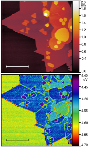
Scanning tunneling microscopy, Kelvin probe force microscopy, and transmission electron microscopy were used to obtain high resolution images and quantitative measurements of the local density of states, work function and nature of defects in MoS2 films. We track the evolution of defects that are formed under heating and electron beam irradiation. We observe formation of metastable domains with different work function values after annealing the material in ultra-high vacuum to moderate temperatures. We attribute these metastable values of the work function to evolution of crystal defects forming during the annealing. The experiments show that sulfur vacancies formed after exposure to elevated temperatures diffuse, coalesce, and migrate bringing the system from a metastable to equilibrium ground state. The process could be thermally or e-beam activated with estimated energy barrier for sulfur vacancy migration of 0.6 eV in single unit cell MoS2 . Even at equilibrium conditions, the work function and local density of states values are strongly affected near grain boundaries and edges. The results provide initial estimates of the thermal budgets available for reliable fabrication of MoS2 -based integrated electronics and indicate the importance of defect control and layer passivation. For more details please review the article published in Scientific Reports.


