Hardware pages: where the bits meet the metal.
Back in 2007 I submitted a patch to Comedi to support triggering analog output off the analog input start signal. The patch was accepted, and is now old news, but I just ran across my notes from developing it, and thought I'd publish them for posterity (and as a reminder to myself in case I have to dig into the internals of Comedi or NI drivers in the future).
Patch notes
To understand the patch, you should understand some portion of National Instrument's Data Acquisition Systems Timing Controller (NI DAQ-STC, see “Understanding NI DAQ-STC” below and the manual for more details).
We are trying to set up the AO timing so it triggers off of the AI
start signal. In NI terminology, that means we want AI_START1 to be
the source of AO_START1. The possible sources are listed in the
DAQ-STC manual in table 5-2, p6-7 (380), where we see that
AO_START1's 19th input is AI_START1. To implement this, we need
to write to the card's AO_Trigger_Select register (Appendix B,
register 67, pB-21 (470)).
Sounds fairly simple, we should just be able to set the appropriate
start_arg. However, looking into source of
comedi/driver/ni_mio_common.c, we see that no external triggering
information is written to the AO_Trigger_Select_register. Looking
back through the STC manual, we come across their AO trigger example
(3.6.1.4, p3-23 (185)) which shows how to set up AO triggering.
Comparing to ni_mio_common.c, we see that the AO triggering
configuration in ni_ao_cmd() looks just like the “software
triggered” case in NI's example. So it seems impossible to run
externally triggered AO.
The patch edits ni_mio_common.c to make it more like NI's example
and ni_mio_common.c's own AI code.
Understanding NI DAQ-STC
Consider the timing sequence shown in the Comedi manual. For output, all the same timings apply, but data is flowing the other way.
Here is a translation table between NI's terminology and Comedi's (NI references from STC manual):
| Comedi AI | NI AO | Reference |
|---|---|---|
| seq_start | AO_START1 | Fig 3-10, p3-12 (174) |
| scan_begin | UPDATE | Fig 3-2, p3-6 (168) |
| convert | TMRDACWR | Fig 3-2, p3-6 (168) |
There are references to an AO_START as distinct from AO_START1,
but it appears to be unsupported:
- It does not show up in the manual's AO feature list (section 3.2, p3-2 (164), compare to the AI feature list, section 2.2, p2-2 (31))
- It shows up in some contexts as unsupported (e.g. section 3.6.5, p3-36 (198))
Comedi is a Linux COntrol and MEasurement Device Interface. We use Comedi in our lab to contol experiments via a NI PCI-6052E. The basic architecture for a Comedi application is:
kernel space   |   user space
               |
device         |
  |            |
kernel --------|-- libcomedi - application
  |            |
comedi module  |
To make matters more complicated, there are two version of the kernel module, one in Git at comedi.org and another in the kernel itself.
Luckily, many distributions now package versions of the in-kernel staging driver (e.g. Debian and Ubuntu). I was feeling left out on Gentoo, so I've just revived the old Gentoo packages and added them to my Gentoo overlay.
Relying only on the measured deflection voltage to measure the AFM tip-surface interaction is risky, as the loss of the signal may not be obvious. In order to validate incoming photodiode signals, you should also monitor the total light hitting the photodiode. This is especially true in fluid cell measurements, as bubbles of air or buffer solution can deflect the laser enough to miss the photodiode completely.
As far as I can tell, the total photodiode voltage is not carried on one of the DB-25 lines connecting the MultiMode to the NanoScope controller (see the MultiMode internals page). It is displayed on the MultiMode LCD, so I monitored the lines connecting the main board to the LCD board to isolate the total photodiode line (LCD connector 2). I build a small connector to tap out that line (despite appearances, none of the huge solder blobs actually short anything out :p).
TODO: image of connector.
We sent the tapped line out through Auxilliary D (DB25 line 4), so we could tap it again at out main break-out box. Comparing this signal to the photodiode ground (DB25 line 12), the signal is actually inverted (-7V signal when there's lots of light, 0V when there's none).
Here are my current guesses about the role of various connector lines inside the MultiMode II
DB-25 line descriptions
| DB-25 line | Role | To |
|---|---|---|
| 1 | Stepper A | Main 3 |
| 2 | Stepper B | Main 20 |
| 3 | +5 Volts | Main 7 (also 1,2,18,19 through 20 Ohms) |
| 4 | Auxiliary D (role?) | Jumper 2 |
| 5 | HV to piezo (-Y) | Piezo 5 |
| 6 | NCAFMJM pin 2 (role?) | Main 8 |
| 7 | HV to piezo (-X) | Piezo 9 |
| 8 | Piezo/head chassis ground | Peizo 1; Head 13; Jumper 8 |
| 9 | -15 Volts | Main 26 |
| 10 | Analog 2 (gain select) | Main 17, Jumper 6 |
| 11 | Vertical cantilever deflection | Main 15 |
| 12 | Green loop (photodiode ground?) | Main 27 |
| 13 | BB2107 pin 5 (2+) though R (role?) | Main 9 |
| 14 | Manual switch mode AFM/LFM (+5 Volts?) | Switch 10 |
| 15 | Stepper C | Main 4 |
| 16 | Stepper D | Main 21 |
| 17 | Head Gnd? | Head 1 |
| 18 | HV to piezo (+Y) | Piezo 4 |
| 19 | Main board ground | Main 5 |
| 20 | HV to piezo (+X) | Piezo 8 |
| 21 | Horizontal deflection | Main 33 |
| 22 | HV to piezo (+Z) | Piezo 6 |
| 23 | NCAFMJM pin 3 (role?) | Main 25 |
| 24 | +15 Volts | Main 10 |
| 25 | AD620 pin 2 (in -) through R (role?) | Main 31 |
Main board line descriptions
| Main line | Role | To |
|---|---|---|
| 1 | Stepper C, from DS3658N pin 6 | Stepper Black |
| 2 | Stepper A, from DS3658N pin 1 | Stepper Brown |
| 3 | Stepper A? in | DB-25 1 |
| 4 | Stepper B? in | DB-25 15 |
| 5 | Main board ground (black loop) | DB-25 19 |
| 6 | Manual stepper switch direction | Switch Purple |
| 7 | +5 Volts | DB-25 3 |
| 8 | NCAFMJM pin 2 | DB-25 6 |
| 9 | through R to BBOPA2107 pin 5 (+2) | DB-25 13 |
| 10 | +15 Volts | DB-25 24, Head 5 though 10 Ohms |
| 11 | Photodiode D | Head 11 |
| 12 | Photodiode A | Head 9 |
| 13 | DG403 pin 10 | |
| 14 | internal plane, but not ground loop? | |
| 15 | Vertical cantilever deflection 620 pin 6 (out) | DB-25 11 |
| 16 | DG403DJ pin 6 | DB-25 11 |
| 17 | Gain select DG 419pin 6 (through R) | DB-25 10 |
| 18 | Stepper D, from DS3658N pin 8 | Stepper Orange |
| 19 | Stepper B, from DS3658N pin 3 | Stepper Yellow |
| 20 | Stepper C? in | DB-25 2 |
| 21 | Stepper D? in | DB-25 16 |
| 22 | AD827(far) pin 7 (out) (Tapping-piezo voltage) | Head 15, tipholder 6 |
| 23 | Green loop | Head 14 |
| 24 | Manual stepper switch enable | Switch grey |
| 25 | NCAFMJM pin 3 | DB-25 23 |
| 26 | -15 Volts | DB-25 9, Head 7 through 10 Ohms |
| 27 | Green loop | DB-25 12 |
| 28 | Photodiode ground (green loop) | Head 2 |
| 29 | Photodiode C | Head 10 |
| 30 | Photodiode B | Head 8 |
| 31 | AD620 pin 2 (in -) through R | DB-25 25 |
| 32 | BBOPA2107 pin 1(out1) through R(total photodiode) | |
| 33 | DG403 pins 1 and 3 (drains from 1)(Horizontal deflection) | DB-25 21 |
| 34 |
Chip list
(following this numbering)
| Index | Chip | Description | Role |
|---|---|---|---|
| 1 | DS3658N | Current sink. | Stepper motor current sink |
| 2 | H7555IBA | CMOS timer. | Manual stepper motor control clock |
| 3 | "NCAFMJM" | ? | Stepper motor |
| 4 | AD827JN | Dual op amp. | Far side amplifies tapping piezo signal (out Main 22) |
| 5 | Scratched out | ? | Stepper motor? |
| 6 | Scratched out | ? | Stepper motor? |
| 7 | AD534KD | Difference multiplier (X1-X2)(Y1-Y2)/(10V)+Z2. | Photo-diode? |
| 8 | AD734BQ | Identical to AD534, but with control over denominator. | Photo-diode? |
| 9 | SG531P 25.0000 M | 25 MHz crystal oscillator. | Photo-diode? |
| 10 | BBOPA 2107AU | Dual op amp. | Photo-diode? |
| 11 | DG419DJ | CMOS analog switch. | Photo-diode? |
| 12 | DG403DJ | CMOS analog switch. | Photo-diode? |
| 13 | AD534JD | Identical to AD534KD, but with slightly more error. | Photo-diode? |
| 14 | AD637JD | RMS-to-DC converter. | Photo-diode? |
| 15 | AD620AR | Instrument amplifier. | Photo-diode? |
| 16 | BBOPA 2604AU | Op amp. | Photo-diode? |
| 17 | DG411DJ | Quad CMOS analog switch | ? |
Main board wiring
Vertical deflection (Main line 15) comes from pins 6 and 8 (shorted together) of the DG403 switch. Pin 6 drains pin 5 and pin 8 drains pin 9 when the switch is turned on. I'm not sure what pin 5 is attached to. Pin 9 is connected (through a resistor) to the output (pin 12) of AD534a.
Manual switch connector line descriptions
See my switch notes for details on understanding the stepper control switch.
| Line | Color | Role | To |
|---|---|---|---|
| 1 | Orange | Laser LED ? | |
| 2 | White-red | STM mode LED | DB-25 17 |
| 3 | Green | Mode TM | Main 13 |
| 4 | Blue | Mode STM | 120 Ohms to DB-25 17 |
| 5 | Purple | Stepper direction | Main 6 |
| 6 | White-brown | Stepper switch +5 Volts | Main 7 |
| 7 | White | Laser LED? | DB-25 17 |
| 8 | Yellow | Laser LED? | |
| 9 | White-brown | STM mode LED | 160 ohms to DB-25 17?? |
| 10 | Red | Mode AFM/LFM, +5 Volts | DB-25 14 |
| 11 | Grey | Stepper enable | Main 24 |
| 12 | Black | Stepper switch Gnd | Main 5 |
AFM head micro-D 15 connector line descriptions
outside female from top-left: 8 7 6 5 4 3 2 1/15 14 13 12 11 10 9
inside male (on board) from bottom-right: 8 7 ... 1/9 10 11 ... 15 blank
| Line | Role | To |
|---|---|---|
| 1 | Laser Ground | DB-25 17 |
| 2 | Photodiode ground | Main 28 |
| 3 | +5 Volts Laser Power | no main, no DB-25 ?? |
| 4 | ||
| 5 | +15 Volts | DB-25 24 through 10 Ohms |
| 6 | STM current? | Jumper 1, tipholder 2 |
| 7 | -15 Volts | DB-25 9 through 10 Ohms |
| 8 | Photodiode B | Main 30 |
| 9 | Photodiode A | Main 12 |
| 10 | Photodiode C | Main 29 |
| 11 | Photodiode D | Main 11 |
| 12 | AFM tip | Jumper 3, tipholder 4 |
| 13 | Chassis ground | DB-25 8, Jumper 8 |
| 14 | Tapping-piezo ground (main board shorts to photodiode ground) | Main 23, tipholder 5 |
| 15 | Tapping-piezo voltage | Main 22, tipholder 6 |
(see, e.g. Glenair for Micro-D-Subminiature connector descriptions.)
AFM head to tipholder line descriptions
Labeled looking down on tipholder along laser, with MultiMode LCD at bottom from top-left: 1 2 3/4 5 6
| Line | Role | To |
|---|---|---|
| 1 | +12 Volts | ? |
| 2 | STM current? | AFM connector 4 |
| 3 | -12 Volts | ? |
| 4 | AFM tip? | AFM connector 12 |
| 5 | Ground | AFM connector 14, main 23, main board shorts to photodiode ground |
| 6 | Tapping-piezo voltage | AFM connector 15, main 22 |
On our tapping-in-air tipholders, removing the connector-pad plate shows lines 1-4 are not connected to anything. Lines 5 and 6 have wires heading over towards the piezo, as you would expect. On our tapping-in-fluid tipholders, the pad is not removable, but the only wires leaving the pad area connect to the oscillating piezo region, so both tipholders have identical interfaces to the head, with 5/6 providing piezo oscillation and 1-4 as non-contacts.
Since both tapping mode pins are shorted through the head to the main board, but not to the DB-25 connector to the NanoScope, we assume the tapping oscillation is being generated on the MulitMode main board itself.
Piezo connector line descriptions
outside male from top-left: 1 2 3 4 5/6 7 8 9
inside male (on board) from top-left: same + blank
DB-25 labeled HV: 5,7,18,20,22
| Line | Role | To |
|---|---|---|
| 1 | Ground | DB-25 8, Jumper 8 |
| 2 | no db | |
| 3 | no db | |
| 4 | +Y piezo | DB-25 18 |
| 5 | -Y piezo | DB-25 5 |
| 6 | +Z piezo | DB-25 22 |
| 7 | Piezo cap | Jumper 7 |
| 8 | +X piezo | DB-25 20 |
| 9 | -X piezo | DB-25 7 |
Jumper pin descriptions
inside male from top-left: 1 2 3 4 5 6 7 8
Roles from MultiMode manual, 14-9
| Pin | Role | To |
|---|---|---|
| 1 | STM current | Head 6 |
| 2 | Auxiliary D | DB-25 4 |
| 3 | AFM tip | Head 12 |
| 4 | Analog 2 | DB-25 10 |
| 5 | Gain Select | Main 17 |
| 6 | Analog 2 | DB-25 10 |
| 7 | Piezo Cap | Piezo 7 |
| 8 | Ground | DB-25 8, Piezo 1, Head 13 |
LCD connector descriptions
inside male from top-left: 1 2 3 4 5 / 6 7 8 9 10
| Pin | Role | To |
|---|---|---|
| 1 | Manual switch AFM/LFM, +5 V | DB-25 14 |
| 2 | Total photodiode voltage | Main 32 |
| 3 | -15 Volts | Main 26 |
| 4 | +15 Volts | Main 10 |
| 5 | Manual switch STM mode | Switch 9 |
| 6 | Head Gnd? | DB-25 17 |
| 7 | Main 16 | |
| 8 | Green loop | Main 27, DB-25 12 |
| 9 | Main 13 | |
| 10 | Horizontal deflection | Main 33 |
LCD board
inside male from top-left: 1 2 3 4 5 / 6 7 8 9 10
| Pin | Role | To |
|---|---|---|
| 1 | +5 V | Big regulator |
| 2 | Total photodiode voltage | |
| 3 | -15 Volts | |
| 4 | +15 Volts | |
| 5 | Manual switch STM mode | |
| 6 | Head Gnd? | |
| 7 | Main 16 | |
| 8 | Ground | Black loop |
| 9 | ||
| 10 | Horizontal deflection | top center BBOPA though R |
You may want to see my MultiMode wiring summary.
The manual stepper switch is a double pole double throw (DPDT) switch. I've labeled the contacts below
In my MultiMode, the switch contacts are wired as follows:
- Contacts 1, 4, and 6 are shorted together, and fed by a white-brown striped wire,
- Contact 2 is a purple wire,
- Contact 3 is a black wire, and
- Contact 5 is a grey wire.
Using a multimeter to measure the average voltages I got:
| Wire | Up | Down | Off | Role | Main | DB-25 |
|---|---|---|---|---|---|---|
| Black | 0.2V | 0.2V | 0.0V | Ground | UL+4 | none |
| Purple | 5.0V | 0.2V | 0.0V | Direction | UL+5 | none |
| Grey | 5.0V | 5.0V | 0.0V | Enable | LL+6 | none |
| White | 5.0V | 5.0V | 5.0V | Power | UL+6 | 3 |
So the white and black wires carry power and ground to the switch, and the purple and grey wires carry the switch information back to the electronics. The 'Main' column records the line's lead on the main circuit board in the MultiMode, and the 'DB-25' column records the line's lead on the DB-25 cable to the NanoScope controller.
From the main-connector, the grey and purple lines start spreading out, ending up at (partial list):
- H7555IBA, a CMOS clock.
- NCAFMJM, a top-secret something-or-other.
My guess is that the grey enable-wire from the switch turns on the H7555 timer, and the NCAFMJM is a stepper driver chip, which receives a direction input (the purple wire) and a pulse-to-step input (the H7555 output). The output of the NCAFMJM heads over to a DS3658N current driver which drives the motor.
There is a good deal of drive-train backlash in the stepper mechanism.
Detection procedure
- Step towards surface until there is plenty of surface contact.
- Step away until you leave the surface.
- Repeat until you have too much data :p.

Conclusions
About 47 steps of backlash. Since we never touch the stepper while any critcal surface interactions are going on, simply replace step back 1 step with step back 60 steps, then forward 59.
Supporting evidence
Noise on reversal
When we reversing the stepper (by any means), the movement is “clearly audible” for “a bit” and then becomes “almost silent”.
To give a rough idea, I usually have keep my finger on the drive-shaft to tell if the motor is moving in “almost silent” mode, but can hear the motor from around 5 ft away in “clearly audible” mode. “A bit” is about 0.5 s when controlling the motor using the manual Up/Down switch.
Why
When I joined Prof. Yang's group, the LabVIEW software controlling
the experiment lacked control of the stepper motor which provides
coarse z axis control. This made it difficult to set up the fluid
cell and meant that leaving the system running unattended for over an
hour could place unnecessary strain on the z piezo (as it would need
to compensate for thermal drift on its own).
How
After a staring into the bowels of the MultiMode AFM and watching some of the more suspicious lines on an oscilloscope, I saw that lines 1, 2, 15, and 16 were the stepper motor drive lines and guessed that they were TTL compatible. A short while later (wink), the LabVIEW code was up and running. The LabVIEW computer (via a PCI-6052E card and BNC-2090 box) writes TTL stepper motor currents to the relevent lines on the Nanoscope↔MultiMode cable using our break-in box.
Computer <-> Breakout box <-> MultiMode
NanoScope <------^
Part list (outdated commercial parts linked to the current generation):
- LabVIEW 7.1 (in-house software)
- PCI-6052E
- BNC-2090
- Nanoscope IIIa (altered)
- Homemade break in box
- MultiMode II AFM
Breakout box
Build a DB-25 breakout box, such as the ugly hack job shown below. This gives us access to the stepper motor drive-lines.

Control the motor
First, you need something to write to your new motor control lines. We are using the digital I/O lines from this National Instruments PCI-6052E.
Next, you need to send the proper signals down the lines. Prof. Douglas Jones has an excellent stepping motor tutorial, which explains how to drive a unipolar stepping motor. For basic operation, you just need something like this pseudo-code:
step( up? ) {
  static int index=0; // saved between function calls, only initialized once
  int output[] = {sink 1a, sink 2a, sink 1b, sink 2b}; // the output array
  if (up? == TRUE) {
    index = (index + 1) mod 4;
  } else { // down
    index = (index - 1) mod 4;
  }
  write( output[index] );
}
For my MultiMode, the motor steps 'Up' when I equate:
| DB-25 | Role |
|---|---|
| 1 | 1a? |
| 2 | 1b? |
| 15 | 2a? |
| 16 | 2b? |
Problems
The stepper motor, like any other mechanical linkage, can have problems with backlash.
Figuring it out


General stepper motor wiring
If you look back at the MultiMode interior and main board (above), you can see that there are wires coming from the stepper motor, going into the connector board, and (presumably) ending up at the main MultiMode board. Opening up your own MultiMode (until I get some better pictures up), you will see that the motor has 6 leads: green, brown, black, red, yellow, and orange. A few seconds with your ohm-meter, and you'll find the resistances between the leads are either 20 or 40 ohms. I've recorded the resistances in the following table:
| Brown | Green | Black | Yellow | Red | Orange | |
|---|---|---|---|---|---|---|
| Brown | 20 | 40 | Inf. | Inf. | Inf. | |
| Green | 20 | Inf. | Inf. | Inf. | ||
| Black | Inf. | Inf. | Inf. | |||
| Yellow | 20 | 40 | ||||
| Red | 20 |
Browsing through Prof. Jones' tutorial, we see that our motor is probably unipolar with a total winding resistance of 40 Ohms on each winding.
Looking closely at the stepper motor, you can see (upside down, near
the right hand screw) that it is labeled 5 V DC, and 5 V over a
20 Ohm half-winding gives a current of I = V/R = 0.25
Amps. Following the motor leads back up the the main board (using the
ohm-meter guess-and-check method :p), we find that they come from the
DS3658N (chip 1). This chip takes care of all the details of sinking
the large motor currents given a TTL driving pattern.
WARNING! I strongly suggest you don't do this on your own. The high voltage lines for driving the piezo are potentially dangerous.
The control for the DS3658N was too difficult for me to trace out on the board, so I put the main board back in the MultiMeter (leaving the base-plate off), connected the Multimeter to our NanoScope IIIa, and started clicking on the ‘raise’ and ‘lower’ tip buttons. At the same time, I watched the various DB-25 lines on the oscilloscope. DB-25 lines 1, 2, 15, and 16 oscillated, but only when the motor was turning, so I figured they must be direct TTL controls getting (somehow) to the DS3658N. I built a DB-25 breakout box to take control of those lines, and started writing software.
Line roles
Knowing the stepper control lines and how to control a unipolar motor, it was only a matter of matching the lines to the roles. I arrived at the matches that I pointed out in the How section through trial and error. It was fairly easy to get the motor moving macroscopically, and backlash testing convinced me that the microscopic motion is reproducible and smooth.
Stepsize
We measured the stepper stepsize by stepping the AFM tip closer to surface and sweeping the piezo in after each step. This produced the data shown below.
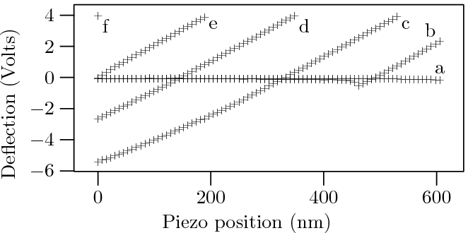
As the motor steps in, we record consecutive traces a, b, c, d, e, and
f. Because we can calibrate the piezo by imaging a calibration sample,
we can convert our piezo voltage into the distance shown on the x
axis. Measuring the x distance between to traces, we see that the
sample moves ~170 nm closer with each step.
Switch
There is a separate post with some details on the manual stepper switch.
The MultiMode product line has been passed through several companies over the years. It started out at Digital Instruments, which was aquired by Veeco in February 1998 before being passed off to Bruker in August 2010.
I've done a good deal of troubleshooting to keep our ancient MultiMode II stumbling along. If you're in a similar situation, check out my notes on:
- Stepper motor control
- Photo-diode signal access
- MultiMode internals
- Closest thing to a description of the NanoScope-MultiMode connection that I can find online. (see Ch. 10)
- A MultiMode manual

Using
Our cluster runs the open source Torque/Maui portable batch
scheduling system (PBS). A batch scheduler takes user submitted
jobs, and distributes them across the the cluster in an intelligent
manner, so users don't need to worry about sharing resources fairly or
sshing into compute nodes to start their jobs. Users submit jobs
to the queue using qsub. I've compiled my own brief
intro to qsub, and there are lots more floating
about the internet.
While PBS queues are great for distributing embarassingly parallel jobs across the cluster, your application may need processes running on seperate compute nodes to share data. A common approach is to use the Message Passing Interface (MPI). Our cluster uses the mpich2 implementation. Cluster-aware applications written in MPI can be started through Torque using an alternate mpiexec from the Ohio Supercomputer Center. There is a nice, brief introduction by Kristina Wanous at the University of Northern Iowa.
Managing
Our cluster (9 dual-core nodes) runs Debian. The compute nodes all boot to NFS roots off the server node. Once that hurdle was passed, setting up Torque, Maui, mpich2, and mpiexec was pretty simple, mostly the usual:
wget ...
tar ...
configure ...
make
make install
with a bit of configuring for our setup. I'll put up some more detailed notes and our config options when I get the time.
GPGPU utilizes the number crunching speed and massive parallelization of your graphics card to accelerate general-purpose tasks. When your algorithm is compatible with GPU hardware, the speedup of running hundreds of concurrent threads can be enormous.
There are a number of ways to implement GPGPU, ranging from multi-platform frameworks such as OpenCL to single-company frameworks such as NVIDIA's CUDA. I've gotten to play around with CUDA while TAing the parallel computing class, and its lots of fun.
With NVIDIA (other vendors are probably similar, I'll update this as I learn more), each GPU device has a block of global memory serving a number of multi-processors, and each multi-processor contains several cores which can execute concurrent threads.
Specs on NVIDIA's GeForce GTX 580:
- 512 cores (16 (MP) ⋅ 32 (Cores/MP))
- 1.5 GB GDDR5 RAM
- 192.4 GB/sec memory bandwidth
- 1.54 GHz processor clock rate
- 1.58 TFLOPs per second
Zoom.
The FLOPs/s computaton is cores⋅clock⋅2, because (from page 94
of the CUDA programming guide) each core can exectute a single
multiply-add operation (2 FLOPs) per cycle. Also take a look at the
graph of historical performance on page 14, the table of device
capabilities that starts on page 111, and the description of
warps on page 93.